GUITAR TUNER
Let’s do the thing hard.
Sorry. I mean do the hard thing.
Until now, everything was on paper and in our minds. We have done some measurements to define requirements, researches about the methods and components to use, designed modules and system, done some simulations and wrote a firmware sketch.
Now it’s time to build the thing. And we start with a prototype.
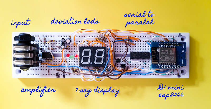
The simplest way to do it is on a breadboard. We don’t have to solder and if we need to do some changes this will be done almost instantaneously (what a long word!).
Actually I did not wrote the FW before the prototype. I only had a basic idea about the modules of the FW. I made the prototype first. The reason is that we may easily do the complete hardware and test modules each on his one (by injecting signals and measuring/visualizing the outputs) but this approach is more difficult with the FW. Therefore, I personally prefer to test the FW by building modules step by step and testing them on the (already build) HW. I start with a basic FW structure and add successive more and more functionality. I check the code/functions first and only if it is OK I go further and add new function. Practically testing the FW modules go somehow hand in hand with the HW test. It’s a wonderful experience of building HW, writing code, testing, doesn’t work, desperation, sleeping over, finding bugs, looking without a clue at the oscilloscope image, finding wrong wiring, still doesn’t work, desperation, sleeping over, making changes, rewriting whole modules, finding more bugs, and finally be proud that it works. Unfortunately you can’t have this wonderful experience as I had it already, before you, and now I give you full functioning schematics and firmware.

My experience has started with this
based on this schematics

From this schematics is missing the by-pass part (output jack and stump switch) cause obvious we don’t need by-pass during debugging and the DC to DC converter with 9V DC jack. For downloading the firmware, debugging and serial monitor we will keep the D1 mini module connected to the PC through the USB. And therefore we will supply the whole circuit from the USB. No need (yet) for the DC/DC converter.
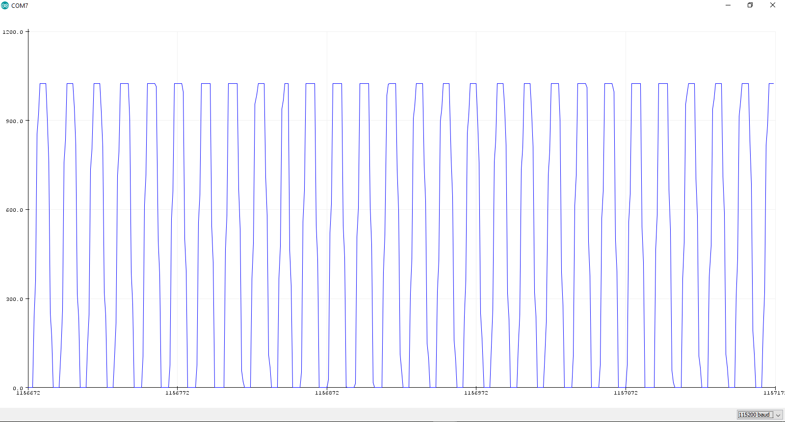
First step is to test the amplifier circuit. We need to feed some signal in the input jack and see what the ESP8266 see. This way we test the wiring of the prototype, the operational amplifier circuit against the simulation and our requirements, the ADC of the ESP8266, communication from ESP8266 to PC and a basic sketch. We may feed the input from a guitar but this will be totally unpractical. (LOL that you even thought about this. YOU FOOL!) We need a constant signal and for start a nice sinus will do. I use an app on my phone. It is called Function generator and may generate two independent signals, out through the stereo headphones jack. I only need to build, using the 3.5mm jack from an old headphones pair, a 3.5mm to 6.3mm jack adapter. You can also buy this adapter, but as I had already both the 6.3mm jack and the old headphones it was easier for me to solder the 6.3 jack to the cable than order it and wait (im)patiently till it arrive. I generate a sinus of 440Hz with the app and this are the signals at the input jack and at the output of the op.amp.
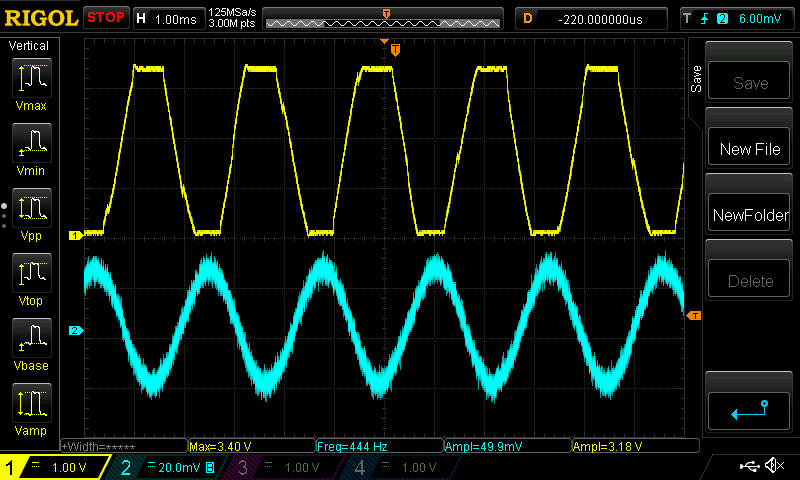
Input signal (channel 2 – blue) has a peak-peak value of 50mV and the op. amp output (channel 1 – yellow) has a peak-peak value of 3.2V (but most probably around 4.5V as the signal is already in overdrive). Note that over driven the signal will not bother us much. An over driven signal has just more and more higher harmonics , but the fundamental is still there. In the extreme case of a square signal there are an infinite of harmonics of decreasing amplitude. But still the fundamental is there and it has the highest amplitude.
The amplification of the circuit is 4.5/0.05 = 90.

That’s not what we have calculated, simulated and wanted! We wanted to have an amplification of 10. Sure we did, but with the electrical guitar, with an output impedance of around 7kΩ. We are using now the headphones jack of the phone and this output impedance is not 7k but almost 0Ω. Therefore we have in the schematics resistors of 470R and 47K for the amplification of the op amp instead of 1k and 82k as in the simulation. I bet nobody noticed the difference! And the measured results above are with 470R/47K. With the initial 1K and 82K the amplification was even higher! Actually out of this component values and measured amplification we may even calculate the output impedance of the headphones output on my phone. The amplification is 47K / (470R = xR) ≈ 90. Results that x ≈ 30Ω. I don’t know. May be right, especially as we have estimated the peak-peak of the op amp output, but I did expected an even lower impedance. Anyhow, all this are not really relevant for our design. I just divagate.
With just enough firmware to acquire data from the ADC (setting the interrupt to read the ADC at constant intervals ; acquiring 1024 samples; send the sample values to the PC through the serial output) I recorded this data at the PC, using the serial plotter in the Arduino IDE and an input signal of 110Hz.
It looks OK. At least it is good enough to find his fundamental frequency of 110Hz.
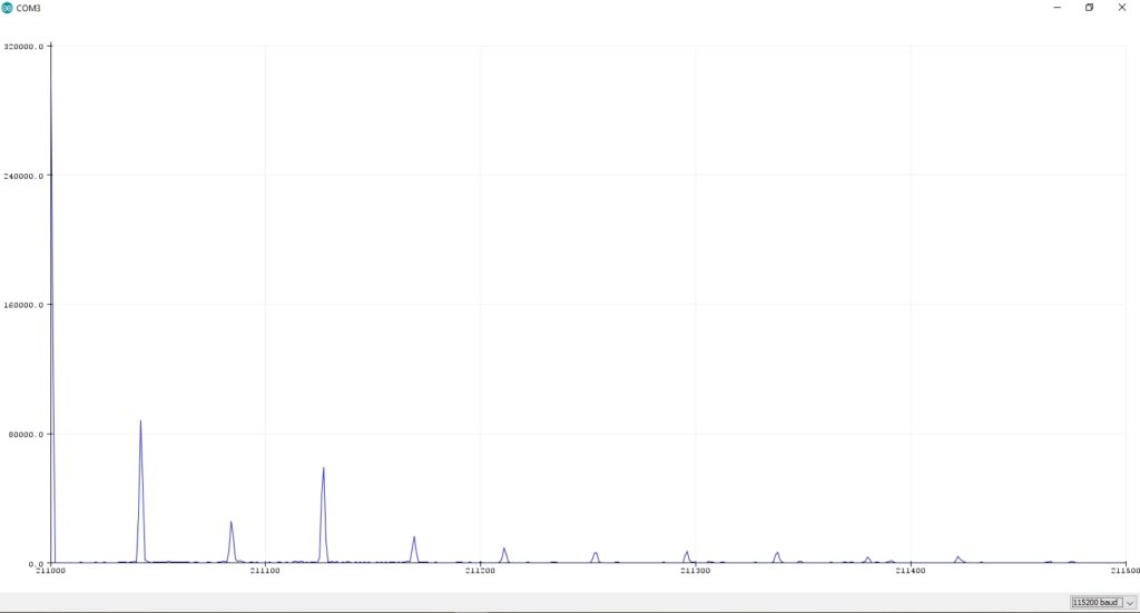
Now that we know that the signal is reaching the ADC and it is converted to digital data properly we add the FFT functions to the Fw . And we calculate the spectrum of the signal and send it to the PC were it is recorded by the serial plotter. Here it is
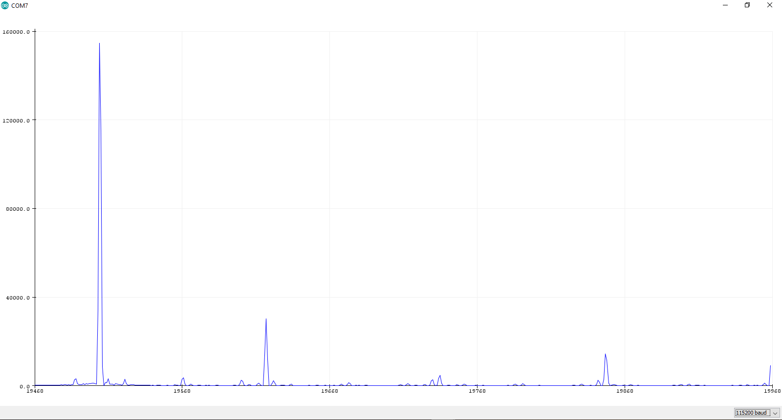
We see clear the main component . Although we can not identify the frequency. Due to the continuous way of working of the serial plotter we see on the x-axis the sample number from the beginning of the recording and not the sample number in the FFT, but believe me that it is 110Hz. We also see that there are some higher harmonics. The third, the seventh and a little from the ninth. Almost no fifth harmonic. The presence of this harmonics is obvious as the input signal is over driven. Actually for presentation purposes I deliberately over driven the signal, so that harmonics are present in the signal.
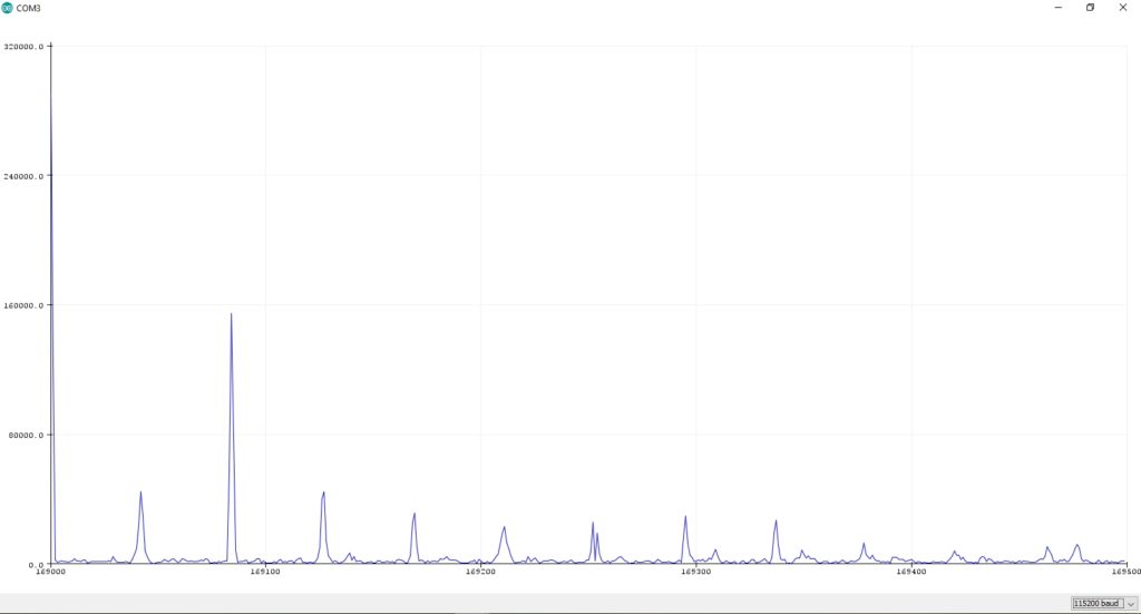
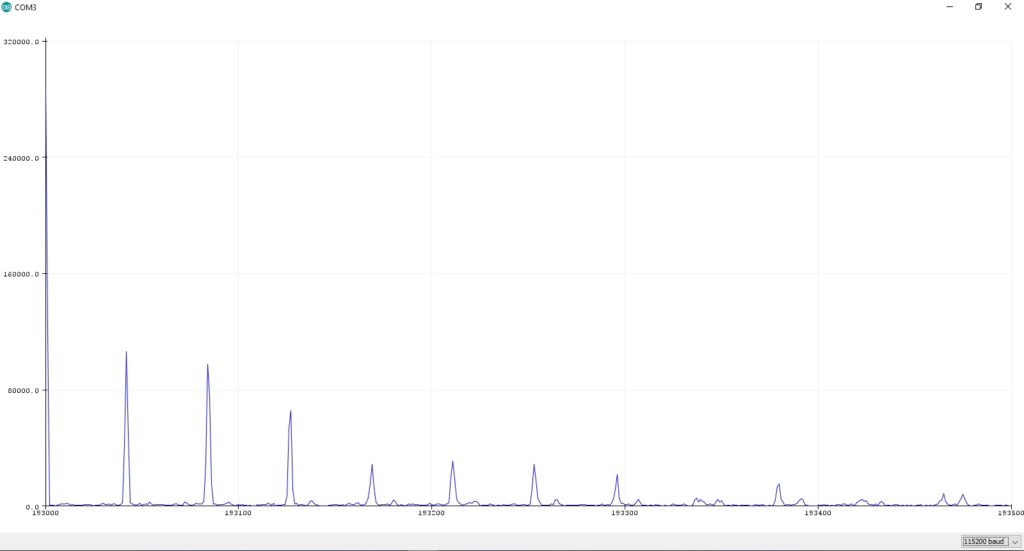
And now to something completely different: The spectrum for an E2 played on the guitar at different moments in time.as computed by the device and displayed on the serial plotter.
At this stage we are half way to the finish.

We just need to determine the local peaks in the spectrum, each one being a harmonic, take only the lowest one as fundamental, make some calculation to interpolate out of the discrete samples the real value in between the samples and that’s it; we are done. In all this process we send for debug purposes data to the PC over the serial monitor. We may insert anywhere and everywhere in the sketch code for data sending to the PC, in order to see if we have got so far in code, and what data we have at that particular place in the code.
To calibrate: we will send a sinus of a precise frequency and look on the serial monitor to see what the device consider to be at the input. The Tone generator app can set the output frequency very fine and it will be quite suitable for this. By doing this for every note from A1 to B5 I have noticed that the device has small errors. The error is not random but systematic. It is always the same for a specific frequency/note and therefore may be compensated by adding (or subtracting) a fixed value from the computation result. The values are different from frequency to frequency. I found the correction values empirically and I put them in a look up table. I am not sure where this errors are coming from. My guess is the curve of the real spectrum. We assumed in the interpolation from discrete to real values, for simplicity, a second order function, but most probably the function is of an higher order. Therefore the small errors. Anyhow, with this correction the results are correct and repeatable.
Out of the calculated frequency, based on a look up table, we get the note. The table is generated at start up knowing the lowest frequency of 55Hz = A1 and the ratio of 1.059463 between every two consecutive semitones (notes). Up to the last note of B1. The ratio is actually the 12th order square of 2. An octave is doubling the frequency (A1 = 55Hz, A2 = 110Hz) and inside an octave we have 11 pitches and therefore 12 intervals, each frequency being the lower note frequency multiplied by this ratio. Just do the math. You will see.

Tthe absolute difference between the calculated frequency and the ideal pitch (from the look up table) will be calculated in relative difference and based on this deviation the LEDs will be switched on/off to indicate in the tuning process how far are we from the ideal pitch.
There is also a look up table for the note name (A,B, …, H) and octave ( 1 to 5) based on the actual frequency.
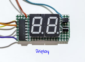
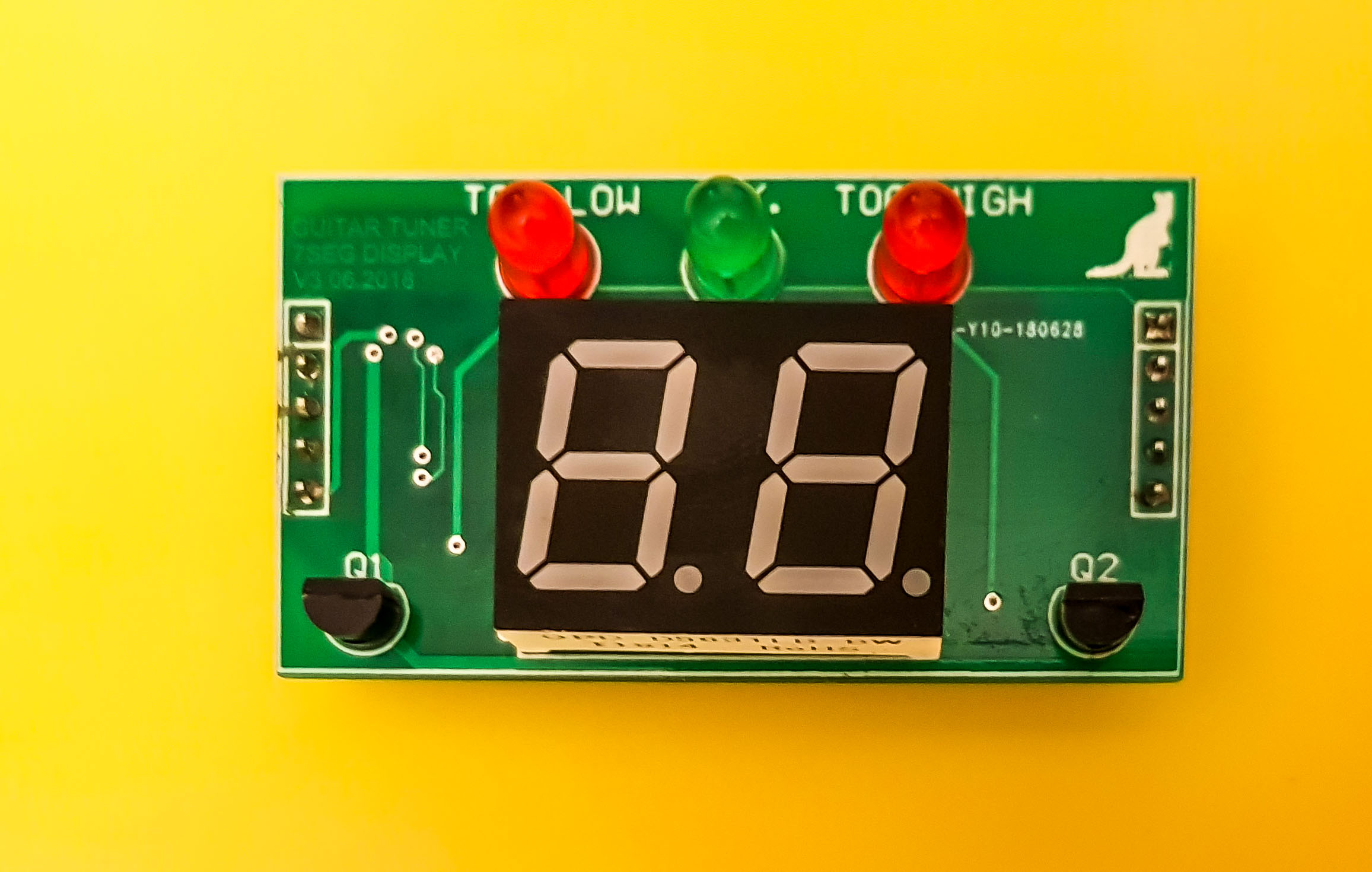
To display the note/octave we use two 7 segments display, multiplexed. Each LED of the 7 segments displays is driven by one output of the serial to parallel converter IC HCF4094. We have to build in the Fw a data byte in which each LED is represented by a bit and then send this byte serially to the HCF4094, with the MSB (Most Significant Byte) first. With a short STROBE signal the serial byte will be output at the parallel output and the LEDs will be switched ON/OFF according the bits in the data byte. We have a look up table to define which bits are 1 and which 0 in order to represent a specific letter from A to H and a specific numerical digit. On the display we have notation “a” to “g” plus the dot (DP) , “a” corresponding to the top segment than going clockwise till “f” equal the segment left-up plus “g” being the segment in the middle and finally the dot. 8 bits in total, “a” being the less significant bit and DP the most one.
A capture of one data byte as send serially.
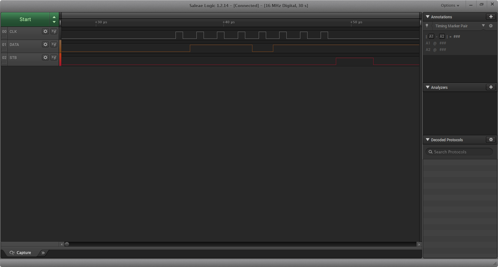
We have the three signals (CLK, DATA and STB). Data is transferred on the rising edge of the CLK. As we send the most significant byte first, we may see that the byte binary value is 01110111 and this is the representation of the letter A.
The display is refreshed in the same interrupt as the data acquisition take place, and therefore we have a change of the display every 0.5ms. At every change we send the data either for note or for the octave and we switch the power for the corresponding display accordingly so that only the correct one should lit till a new byte will be send.
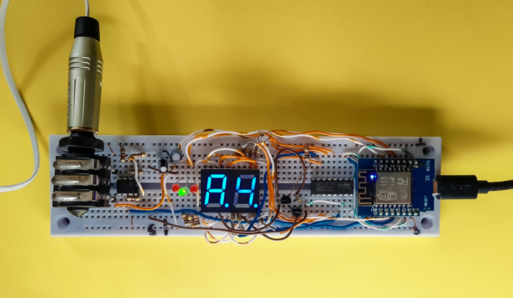
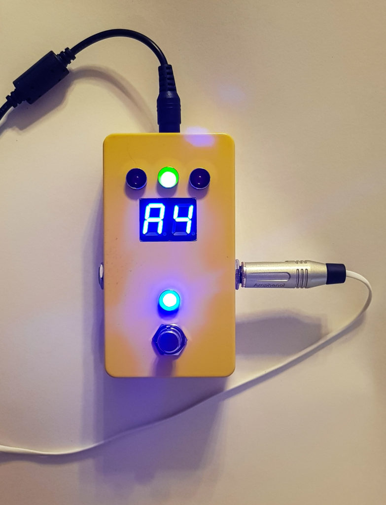
Here is the final result, detecting A4 as ideal pitch.
Now that the prototype is working, we will make a nice PCB, a nice case and to will test it in the real world, with an electric guitar.
First I did a second prototype in a metal case. A case like any other guitar pedal. It was without a real PCB. Just components soldered on breadboard. But it was awful tight. Full of wires.
Well, not quite like this masterpiece, but anyhow.
The most space is being taken by the stump switch and the two audio jacks. And the openings in the metal case have been done by hand and are far from perfect. It works, but it was not the eye catcher I wanted.
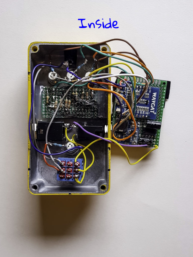
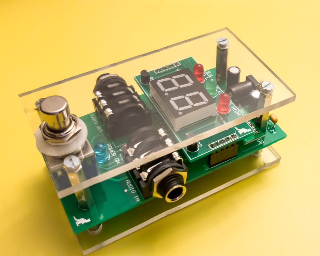
As I said, it works but has a lot of flaws. The main one being that it is no eye catcher. It’s just to “mainstream”. Therefore I had the idea to put everything in-between two transparent acrylic plates. Then everything inside will be visible. It will be cool. But, because it will be visible, everything inside has to be clean and nice and good looking. we can get away with components soldered on breadboard and wires lying all over around. The circuit has to be on a PCB.
Again, what are the requirements (and benefits) for this implementation? We are not talking about the circuit or the firmware, cause those are already fixed, but about the practical realization. And there are most mechanical thoughts and constraints.
- We still want similar dimensions as for the metal case one. This means that we don’t have enough space to put everything on one single PCB. As in the case of the metal case realization from above , we will have to split the circuit. The 7 segment display together with the serial to parallel converter, the two transistors and the three LEDs will be on a small PCB and the rest on a “main”PCB. The two PCBs will be stacked one over the other. Of course the small one will be in top. We will use some similar stacking connectors as the Arduino system does: pin strips.
- The 7 segment display and the LEDs don’t need holes in the upper plate. They will just shine through. And whatever other holes may be needed is much easier to do them in acrylic than in metal.
- The main PC, the upper plate and the lower plate will all have the same dimensions and will be keep together with spacers placed in the four corners. Metal spacers, cause they shine nice. We will use two sets of spacers. One between the lower plate and the PCB and the other between the PCB and the upper plate. At the PCB level the two sets of spacers will go one inside the other if we use one set of spacers with thread pin and the other with thread hole. At the plates sides the spacers will have thread inside. We will fixed the spacers to the plates with screws (or the other way round, depends how you see it).
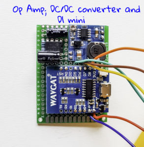
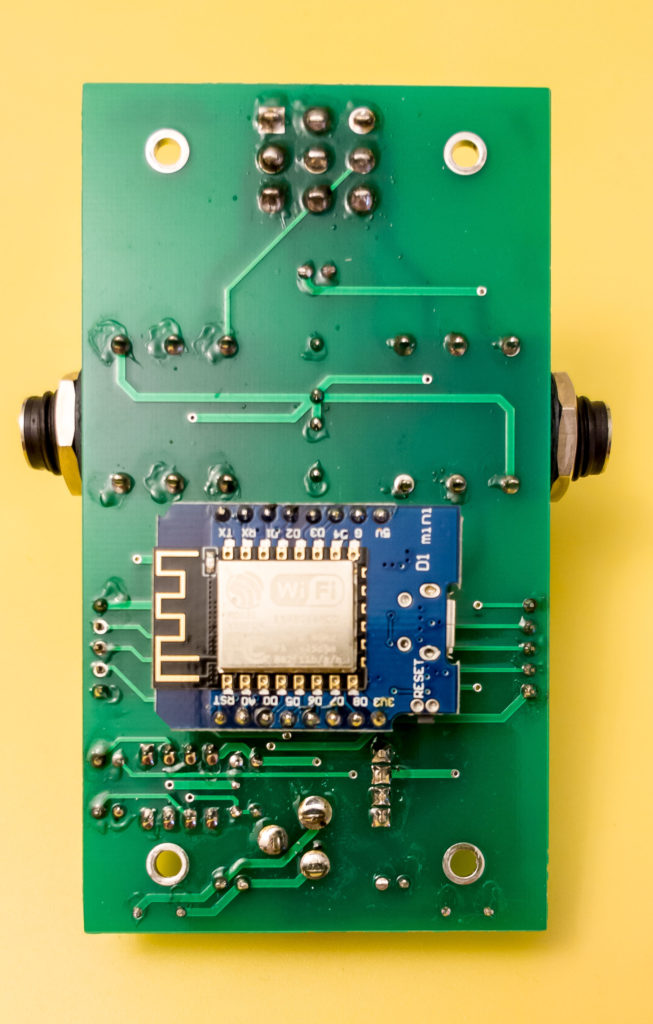
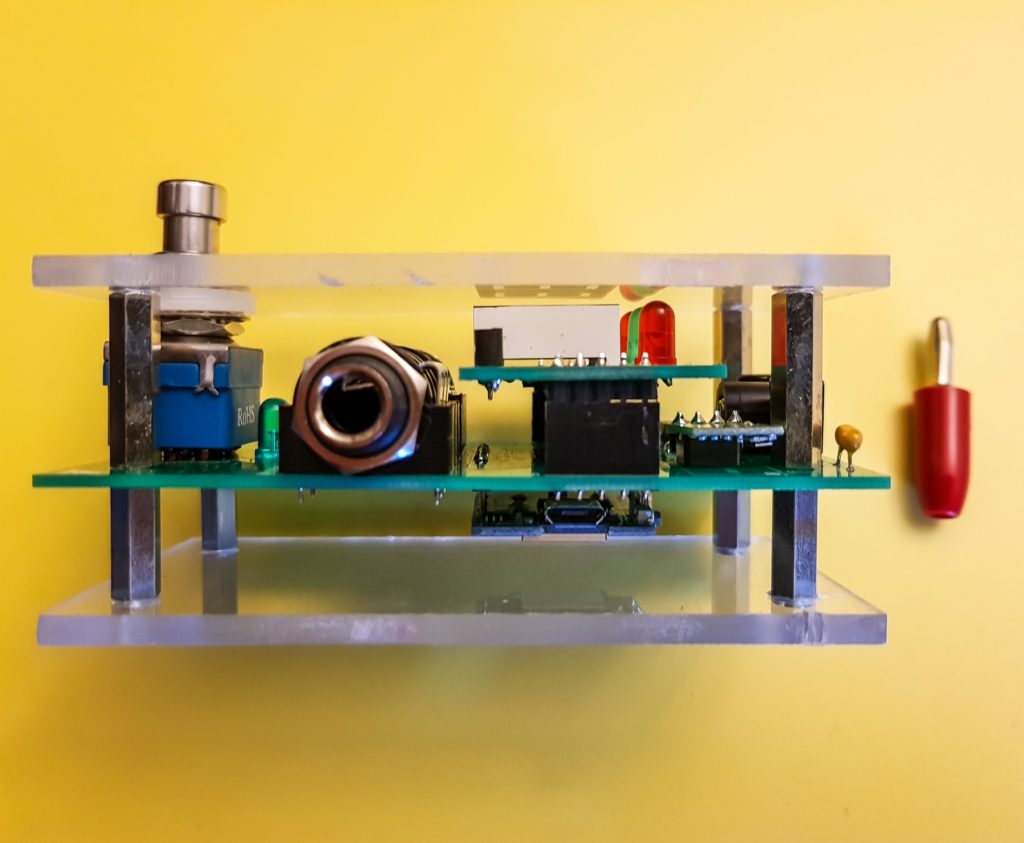
- To save space we may use the main PCB on both sides. If we place the Wemos D1 mini module on the upper (front) side of the PCB, beneath the display PCB we will probably not be able to access the USB port on the module. We need to place the D1 module on the lower (back) side of the main PCB.
- No plates on the sides. Just the upper and the lower plate. Why? Because it will be more difficult to make a complete enclosure out of the acrylic plate and “airy” will look even cooler.
- As there are no plates on the sides, the two 6.3 mm jacks and the DC power jack will just be soldered on the PCB, without any other fixing.
- The stomp switch is still needed. No other way to switch ON/OFF on stage. It will be soldered on the PCB and, in order not to damage the PCB when pushed (by foot!), it will be additional fixed with screw-nuts on the upper plate. This way it will not bend the PCB beneath as the main stiffness is given by the acrylic plate. The acrylic plate has to be stiff enough , so we use 4 mm thickness ones. The switch has a thread between his body and lever. We will put a screw-nut bellow the upper acrylic plate and one above it in order to fix the switch. Therefore the spacers between the main PCB and the upper plate is as long as the stomp height from PCB to the thread (for the switch that I choose this is roughly 16 to 26 mm depending where we put the nut) plus the screw-nut thickness (0.5mm?). As we screw the switch on the other (the upper) side of the upper plate too , we need to take away from the switch thread length the thickness of the acrylic plate (4mm). So we have a height of 16 to 22mm . The standard spacers are coming only in some standard heights. Luckily 20mm is a standard length.
- The pin strips for the connection between the two PCBs, can not be very high as we need to keep the 7-segment display and the LEDs still bellow the upper plate. The height of the pin stripe female + male plus small PCB thickness (1.6mm) plus 7 segment display thickness (8mm for the 0.56″ ones that I choose) must be smaller than 20mm. This means that the pin stripe couple must be less then 10 mm.
- All other components will most probably fit inside this 20 mm height.
- On the back side of the main PCB there will be only the D1 module which is rather low so the spacers there can be only 10 or 15mm long. Not to long cause there is mostly air and it will look strange with longer spacers.
Having all this settled I designed the circuit properly for a layout.

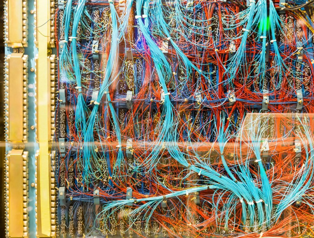
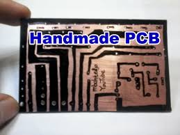
Don’t be fooled by this picture. This is just a stock photo. That’s the way the world, including a photograph, thinks that electronic engineers and hobbyists are doing the circuits. In reality it’s more like this (thank you mbahtedjo @ youtube)
I’ve done the layout and I even ordered PCBs (a pack of ten, cause that’s the minimum quantity you can order).
Bellow are the two schematics and the two layouts. The complete projects may be found as projects in the CircuitMaker Workspace. The projects are called: “Guitar Tuner – Main PCB” and “Guitar Tuner – Display PCB”. The CircuitMaker workspace is a cloud based design system. You must be registered (it’s free) and it will let you download, modify and use any project from this cloud workspace. CircuitMaker is made by the same company who did Altium Designer and it is based on Designer. In return of having a good PCB program for free and without limitations , you must upload your own designs in cloud and made them accessible for the whole community. There are Pro’s and Con’s to this approach, but that’s the way it is.
For those who don’t want to do the whole process of registering, here is the complete documentation (except for the Gerbers)
- Main PCB.
Schematics
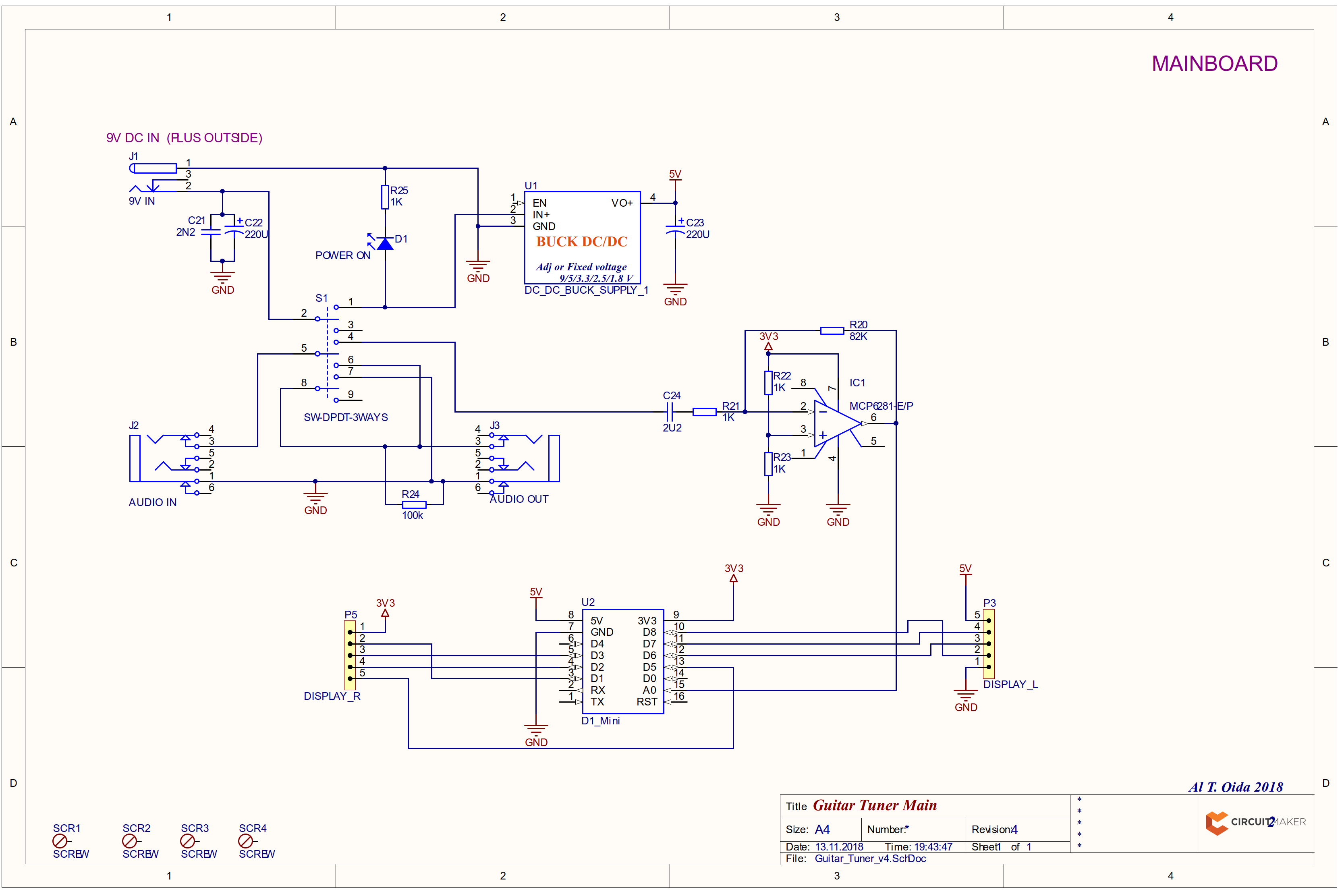
Some comments
- the stomp switch is wired so that :
when switched OFF:
- cut the power supply to device
- directly connect the input and the output
- no signal at the amplifier input.
when switched ON: –
- supply the device
- cut the signal path toward output
- direct the signal toward the amplifier
- there is a 100K resistor (R24) parallel to the output to avoid having a high impedance at the input of the power amplifier stage (this may induce noise, hum , … ), when the device is switched on and there is no connection to the low impedance of the guitar.
- the 5V is made through a DC/DC converter, ready made. There are some buffer capacitors (220uF) and one 2N2 to cut possible high frequency components coming from the external power supply. It is good practice to combine power filters capacitors (in the range of uF) with high frequency filter capacitors (in the range of nF).
- signals going to the both Display connectors are looking funny , but laying them this way has made the routing in the display PCB easier.
PCB layout with assembly and dimensions
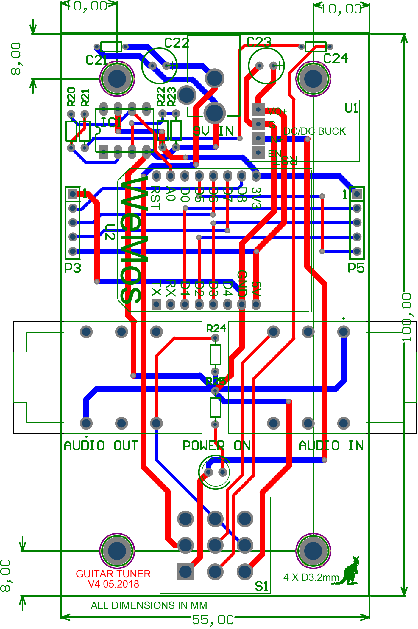
remarks:
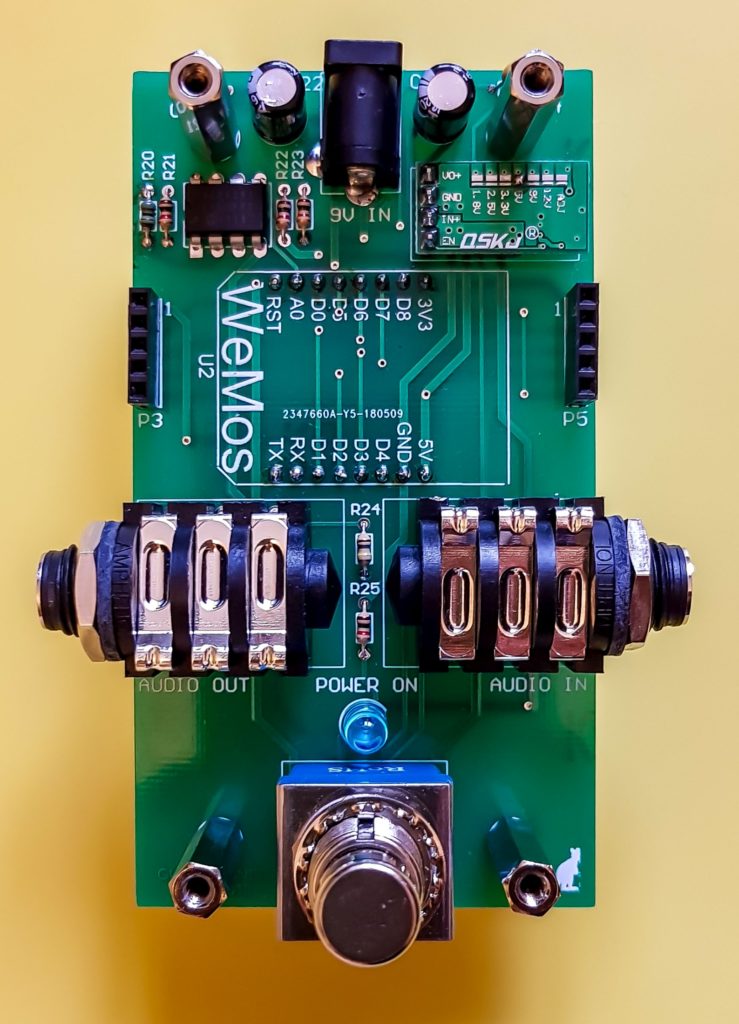
- we have a radial ground net to avoid interference of the analog and the digital paths over the ground tracks.
- Usually , for hand planted components all polarized components (electrolytic capacitors) or components with direction (LEDs, ICs , transistors, diodes, ..) are placed the same way. We avoid mistakes during planting if all capacitors have, for instance, the plus in the same direction. Same for LEDs, ICs, …. . Even if this implies a more complicated and not neatly layout.
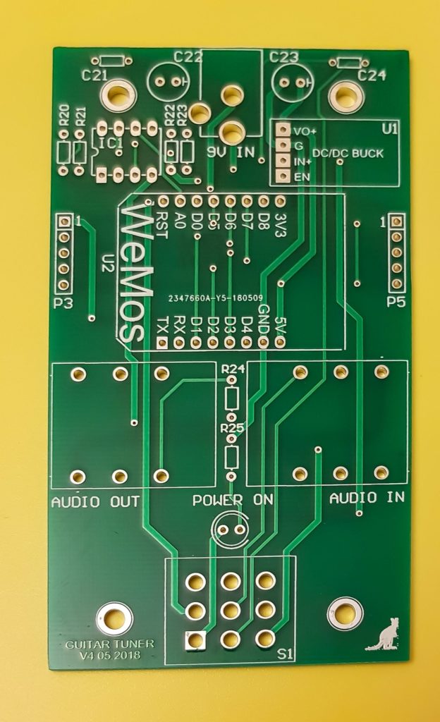
and real PCB (naked, assembled top and assembled bottom)
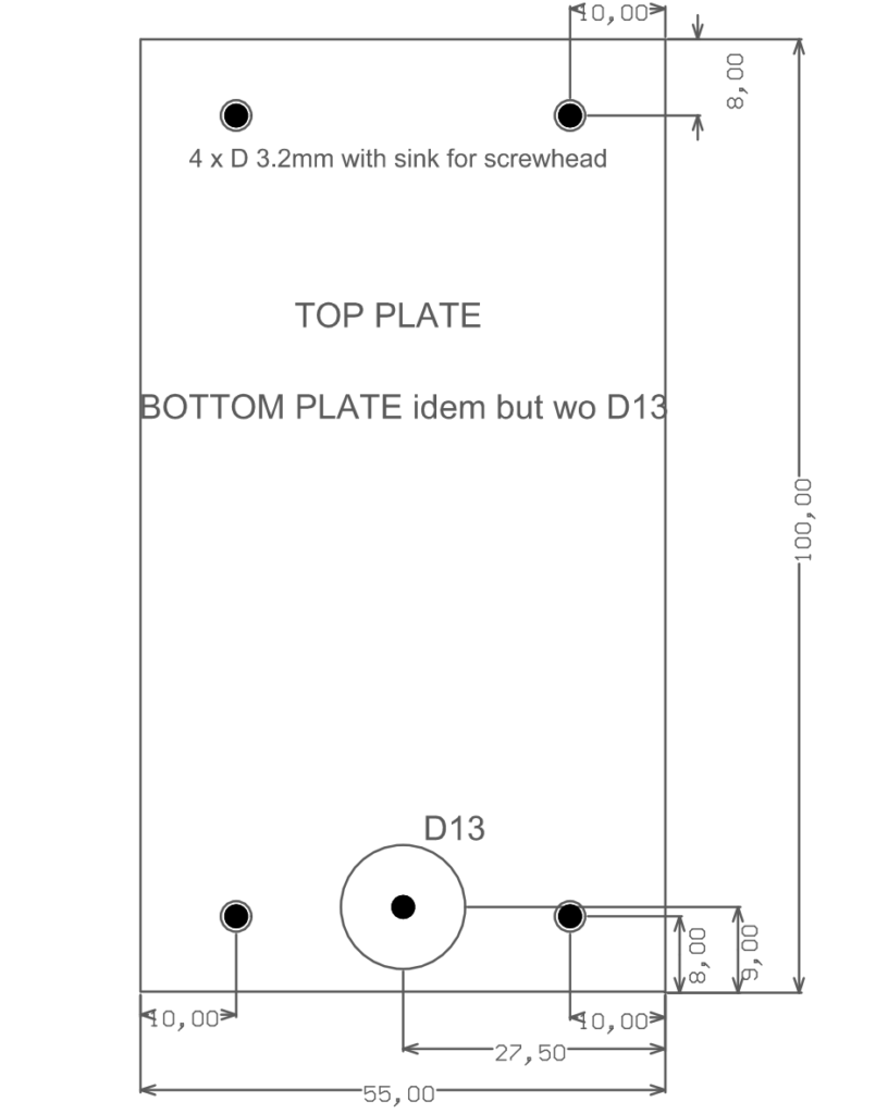
Acrylic plates drawing
Here is the Complete documentation for the main PCB
- Display PCB
Schematics

Nothing much to be said about the schematics. The BSN254A transistors, being obsolete, have been replaced by the similar type 2N700.
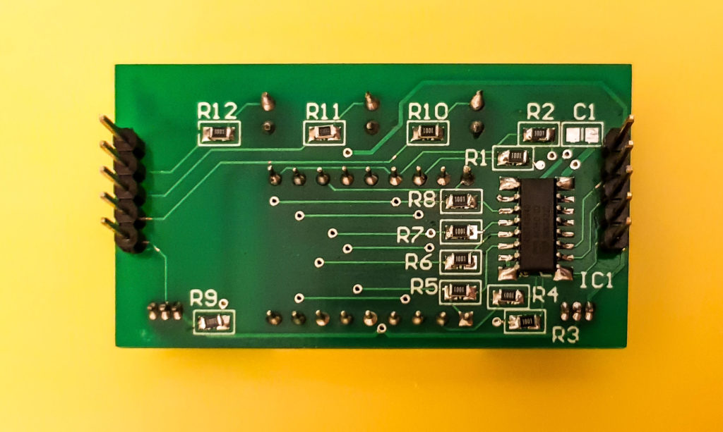
PCB
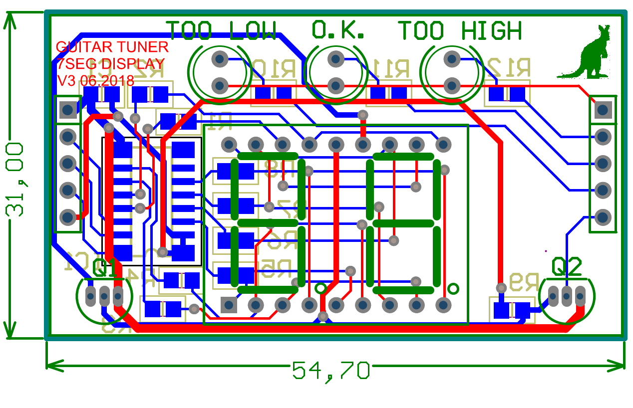
There was not enough space to have the parallel to serial IC and the LED current limiting resistors in through hole type. I was forced to have them in SMD type. But SO16 and 0805 are still OK to be soldered. For me it’s no problem at all and for those with some experience there should be no problem too. As for the rookies it could be an easy way to start with SMD. Actually I don’t know if someone else will want to build this crap. Maybe, maybe not. I don’t really care. (Ye, you got me: if I don’t care why do I spend so much time in writing this explanations??!)
The real PCB (naked, assembled top and assembled bottom)
Complete documentation for the display PCB
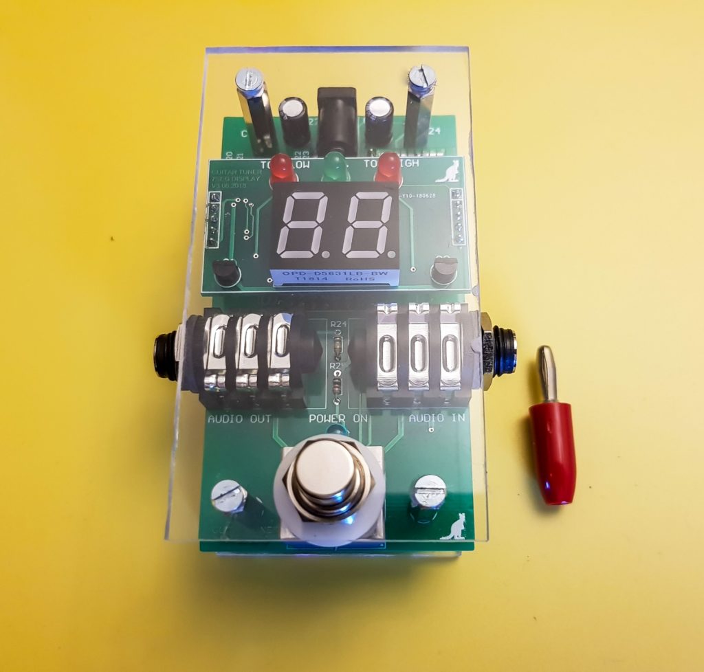
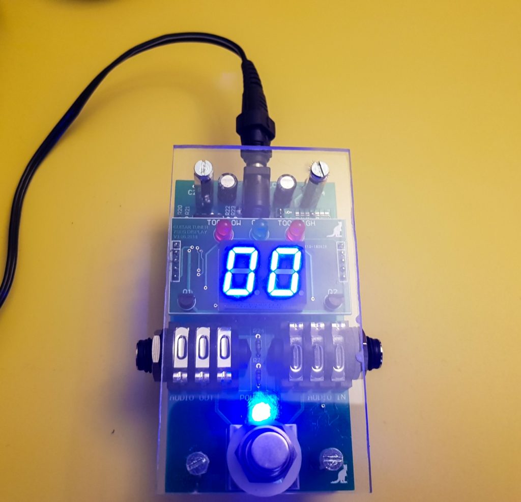
And the complete assembled device (banana for scale)
A short film of tuning a guitar. Well, not “a” guitar, but “the” guitar, as it is the only one I have access too.
That’all.
After some time using the device I can say that basically it is OK. But there are small draw-backs.
- only two refreshes of the data per second is sometimes a little bit slow
- sometimes the octave is shortly wrongly recognized as the higher than the real one. But the note is OK, so this is not really a stop show. After all you know which chord you are tuning and what octave to expect.
What’s next: maybe I will try the YIN method. The problem is that I will need to do almost everything new. It’s not easy so maybe I will do it sometime, or maybe not. We’ll see.