GUITAR TUNER
Let’s choose the HW.
We start by choosing the microcontroller µC cause the values and even the necessity of all other components around him are given mainly by the µC characteristics (like voltage supply, input/output pins voltage tolerance, peripherals already included inside the µC, or not included, characteristics of the peripherals and consequently the necessity to adjust the signal in to and/or out of the µC, ….).
We define the requirements toward the µC, based on what we already know about the system and whatever other constraints or wishes we may have:
- The aim was from beginning to use a processor with support in the Arduino development environment.
- Through hole components (maybe with some small exceptions) in order to be able to solder comfortably at home. At least the processor should be through hole type or a pre-build PCB should be available (like the Arduino boards). If it is a board it should be of small dimensions in order to fit inside a relatively small guitar pedal case.
- FFT algorithm routines should be already implemented for the processor/board.
- ADC should be available inside the µC , with at least 1 channel, 10bit, min 2kHz sample rate.
- Cheap.
The Arduino family itself is not suitable because the processor speed is not high enough to do the FFT calculation on time. At least not in the small boards (Mini, Micro, Nano) which may fit inside our case.
The best solution I come with is to use an ESP8266 board. This processor is actually made for WiFi communications, and this is his strength but we are not force to use it for this. We may use it like any other processor cause it is powerful (RISC with 160MHz), available in the Arduino IDE, very cheap, has an ADC, and there is a sketch for the FFT algorithm. The only issue was with the ADC. The data sheet talks about the resolution of 10bit (that’s good, that’s good) and input range of 0-1 V (good enough). But the sampling rate is practically undocumented. Probably I am dumb cause I was not able to find it.

The data sheet is useless and the internet knowledge is not that vast to include the sampling rate of the ESP8266 ADC. I only found some guy pretending that the maximum sampling rate is 1 kHz , but I seriously doubt that a 160 MHz processor has an ADC of only 1 kHz and I can only guess that he was talking about the speed he was able to read the data in the PC in his specific application. I also found this comment:
“Followup on ADC sampling rate:
– Minimum ADC clock divisor is 8. Therefore, max frequency is 10MHz.
– It takes about 20 cycles to perform a conversion.
– When using fast_read API, assume a conversion time of about 5 us.”
I have no idea how to set the ADC clock divisor. And is the maximum conversion frequency 10Mhz/20 = 500kHz or is it 5us = 200kHz ? Or only 1kHz, as the other guy firmly stated. I am as confused as before

or even more.
The best way to find out was to do my own test. I wrote a small sketch to read the ADC at fixed intervals and send the data to PC via the serial interface. Increasing the frequency of the reading up to 5 kHz has shown no problems. And that’s all I wanted to know cause for this specific project 5 kHz is more than enough.
Now I am gonna tell you a secret.

Actually as I used the ESP8266 before I knew from the start that I will use it for this project too. I only need to check that it will be suitable. But I do keep an open mind for any other solution that may be more suitable.
For instance: the STM32F103 µC it’s a candidate that may do the job. It is an ARM M based µC, with Arduino IDE support, available in small Arduino-like boards, with on internal 10 bit ADC, cheap, … . But comparations with the ESP8266 shows that it is around four times slower. Therefore I am afraid it is not suitable as I am not sure that the STM32F103 will be able to compute the FFT on time (before new samples are available). Although I must admit that I did not try it and I may be wrong

and the STm32F103 may be good enough. On the other hand I am almost sure that it may be good enough to do the YIN algorithm, which I choose not to use this time. But this is, or will be, another story.
There are a LOT of other µCs which may fit. I don’t want to list them all. There are several reasons to not list them.
- I don’t want to do it.
- There are too many
- I don’t want to do it.
- This is not the scope of this page
- I don’t want to do it.
Anyhow, as I used before the ESP8266, I want to use it here too, provided it is suitable. It is very common practice to use for new projects the same µC that one is already familiar with. Cause this will spare you a lot of time. Time that you will have to spend at the beginning (and not only then) in order to understand the characteristics, the performance and the limitations of the IC. Like the existing peripherals, each one with his one characteristics and limitations; the memory map and subsequently some of the limitations imposed on the firmware, including the maximal firmware size; the registers and the assembler commands, in case you want or have to program it in assembler; even the known bugs and work-around. Over time one will have a library for schematics for the processor and for different modules to use with it in different applications. Modules that one has used and know that they work. There will also be different firmware modules one has already tried and knows best. All this knowledge already gained is very precious and it will be a shame not to be used properly.
But sometimes one has to use a new µC in a new project. The reasons may be very numerous and very different. What I want to say is that is efficient to use something you already know but not with any price. Sometimes overall efficiency means to use a new and unknown µC cause it is much better suited for the job. Choosing the “right” µC for the application is a matter of optimizing and compromising.
I can only repeat over and over than engineering means optimizing and compromising in search for the most efficient solution. Whereby “efficient” may be power-wise (low consumption) or money-wise (cheapest) or time-wise (speed of development) or quality-wise (long life and/or low fall of rate) or space-wise (small dimensions) or, or, or…. . Or a combination of them according the specific requirements of the project. Each project may have his one requirements and priorities. For sure designing some electronics for NASA comes with other priorities than designing a low cost high volume mobile phone.

Well , coming back to our design. First conclusion is that we will use the ESP8266 microntroller.
For those of you interested here is the data sheet. For my taste it does not say much. Anyhow as the µC is already mounted on a board with memory and USB to serial. a board which has its own specification, and the Arduino IDE is providing a FFT sketch, there is not much need to know the data sheet. But this is a particular case. Usually one has to read and understand the data sheets (and the errata !).
I will not use the µC as a chip. It is a SMD hardly suitable to solder by hand. It was our requirement to use through hole modules and components, something which anybody may solder at home. Fortunately, as I said, the ESP8266 may be acquired for a couple of dollars as a module with the µC, the program flash and the USB to serial conversion chip. The availability of such module was one of the reasons to choose the ESP8266 in the first place. And there a plenty of modules with the ESP8266. I do not intend to list them all. It will be boring,

and the information may be find in many other places. I choose to use the Wemos D1 mini.
And here is the pinning of the module:
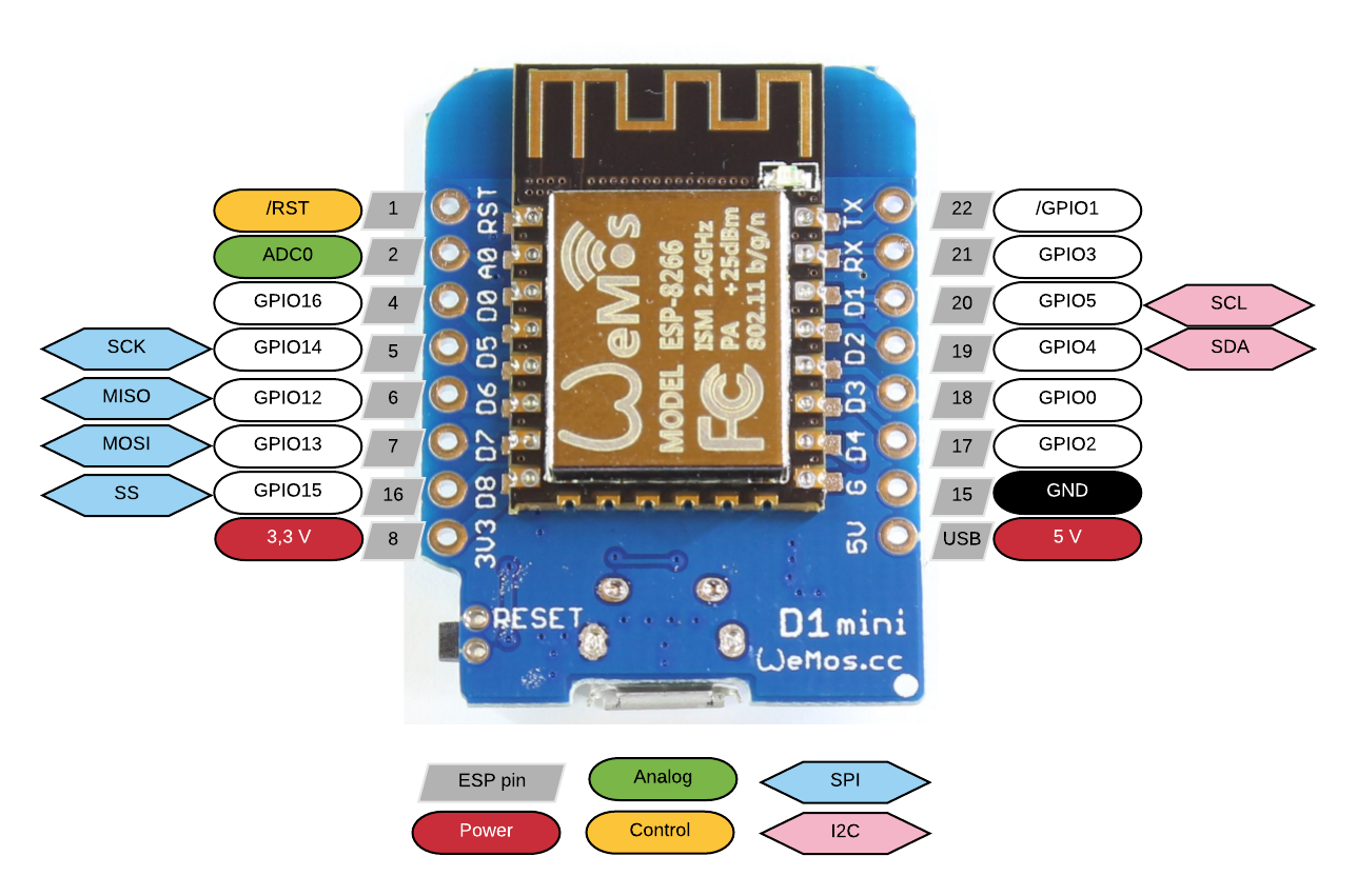
It has 11 general purpose IOs, the ADC, a Reset pin (which I suppose that we will not use), 5V, 3.3V, GND, a Reset button and the mini USB connector, used for downloading the firmware in the chip and data communication with a PC. We will use the USB only to download the firmware and for debug purposes during the firmware development, as the final guitar tuner will be a stand alone device without connection to a PC. The module requires only 5V as supply. The 3.3V is generated internally, through a linear regulator, and it is also on one of the pins to be used externally by other components.
Input signal conditioning
We have seen in the analyze of the guitar signal that the signal amplitude is very low (between some mV and some hundred of mV) and off course it is AC , an “alternative current” signal, going both to plus and to minus voltages in regard to ground. On the other hand our µC of choose has only a plus voltage supply and therefore the ADC can only sense plus voltages. The input range of the 10 bit ADC is 0-1V. The board Wemos D1 mini has already a voltage divider of 220kΩ to 100kΩ between the ADC0 pin of the board and the ADC input of the chip, meaning that the signal at the ADC0 pin of the board may , and should, be between 0V and 3.2V in order to use the complete range of 1V and therefore the whole 10 bits of the ADC.
So we must
- Translate the signal from alternating around ground to alternating around the middle of the ADC input range, which is 3.2V/2 = 1.6V. This way we allow for the maximum amplitude of the signal without clipping either way. This is simply done by coupling the signal through a capacitor of a value big enough to not cut even the lowest frequency we need to sense , this being the note E3 with an ideal frequency of 82.4 Hz. We should take some space toward the lower frequency to allow for tuning in that direction. Let’s choose a frequency of 60Hz. From this upward the signal should not be distorted and his amplitude should be constant and not attenuate.
- Amplify the guitar signal from one hundred of mV to 1.5V . Why 1.5V? Because this is the maximum amplitude we may have , from our new “zero”, which we have choose above to be the middle of the ADC range = 1.6V, toward both the upper limit (3.2V) and the lower limit (gnd), without the signal being clipped either way. Why from one hundred of mV? Because the maximum signal that we expect at the input is around 100-150mV. This for a relatively short period at the beginning. We don’t want to clip the signal but we also want to use as much of the signal as possible, meaning even the small signal toward the end of the vibration should be amplified enough. And this signal is only some tenths of mV or even only some mV. The compromise is to have an amplification of 10. Maybe some signals like E2 will be clipped for a short period at the beginning. But this amplification will also give us useful signals amplitudes for the rest of the vibration. After all the FFT needs as much amplitude as possible to sort the useful frequencies from the noise.
The simplest circuit to fulfill the above requirements is an inverting amplifier with an operational amplifier. It the most simplest amplifier circuit and probably the basic knowledge of any analog electronics engineer. No. Sorry! Of any electronics engineer.
It has to be an operational amplifier with single supply voltage, down to 3.3V, and with both input and output Rail to Rail (the signal can swing all the way both to the ground and the power supply without being clipped and/or distorted). And we don’t actually have to worry about the bandwidth because the frequencies we are dealing are low. Assuming that the highest note we want to tune is C4 that’s around 500Hz, of which the tenth harmonic will be only 5kHz. We also assume that there will be hardly significant levels of higher harmonics than the 10th one. A sampling rate of 10kHz (double the highest frequency) means that we want to have constant amplification up to 10kHz. Together with amplification of 10, this means a gain-bandwith product GBWP of at least 100kHz. (Wikipedia says: The gain–bandwidth product for an amplifier is the product of the amplifier’s bandwidth and the gain at which the bandwidth is measured). Let me tell you that this is not a requirement, but a piece of cake for almost any Op Amp, even from the dinosaur era, not to speaking about the modern ones. Anyhow, almost every Op Amp which is single supply and rail to rail is better than this ridiculous 100kHz GBWP.
I used the MCP6281 from Microchip. The reasons being that it fulfill the requirements and I had a couple of them laying around.
At this point I draw the circuit and do a simulation. I know it is a very simple circuit and there is no reason for a simulation . Every basic electronic book will have plenty of examples and detailed explanations of such one. But I am used to first simulate whatever project I do and besides it is good for practice. There are even Pspice models for the Op Amps of Microchip , including for MCP628x series, but as I use LTspice for simulation , unfortunately this models do not work. I looked in different discussion boards for guys with similar problem. I did indeed found a couple of guys reporting more or less the same problem. But there was no solution. My conclusion is that it has something to do with the differences in syntax between Pspice and LTspice. As I am no specialist of either of them, I had to give up and I looked to find some similar Op Amp model in the LTspice library. After all, for our simple application almost any Op Amp will do, and so will do the simulation too.
By the way, LTspice is a simulation SW. You can find and install it from this address. At least it was on the day I wrote this page. Of course if you are visiting this page in the year 2118 it may have changed in between. I take no responsibility. On the hand if you are really in the year 2118 you probably can figure out on your on.
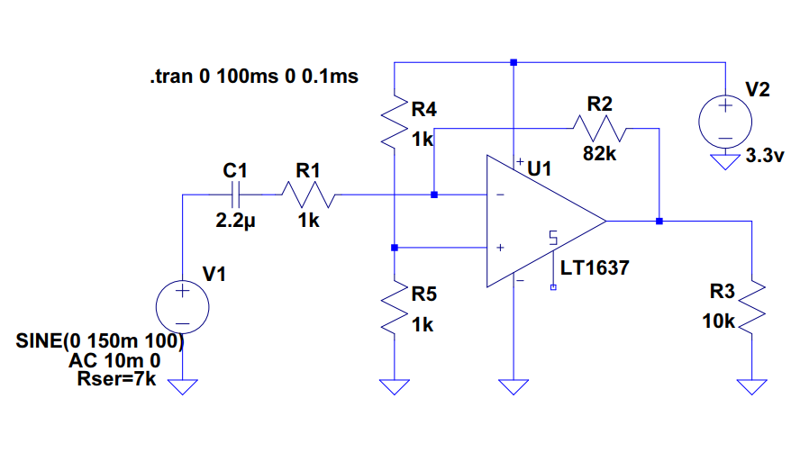
Here is the circuit for those too lazy to draw it self.
Let’s comment a little on the components.
- the Op Amp. is a rail to rail, single voltage, 1MHz bandwidth one. More or less similar to the MCP6281 we want to use.
- the amplification should be given by R2/R1.

A guitar has an internal resistance of the pickup of 6-10kΩ. The voltage source V1 is representing the guitar. I set the internal resistance Rser of V1 to 7kΩ. Therefore for the amplification of the circuit we have to consider the sum of R1 and Rser. The amplification of the circuit is R2/(R1+Rser) = 82k/(1k + 7k) = around 10.
- All resistors are chosen as low as possible to avoid hum. Small currents induced in the circuit due to mains and other parasitic electromagnetic waves will give relatively high parasitic voltages. This is relevant specially at the input of the Op Amp as anything at the input will be amplified by 10 at the output. Therefore we choose R1 only 1KΩ and consequently R2 lower than 100kΩ. And R4 and R5 values are also small enough to limit hum, but still high enough to absorb only relatively small current from the circuit supply voltage. Besides all values are common ones, and in the E12 serie (10%) of tolerances.
The simulation results.
First the Bode diagram (amplification and phase vs. frequency) as result of the AC mode simulation with 10mV input
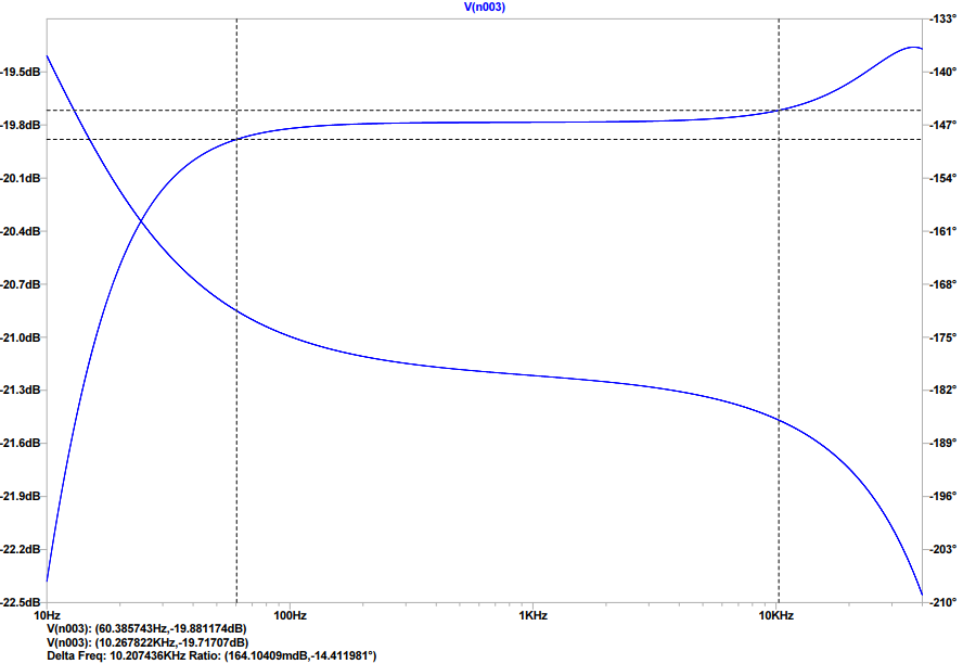
As we see from the cursors, between 60Hz and 10kHz there is only 164mdB = 0.164 dB non linearity of the amplification. For our application good enough.
And now transient response for an input signal of 150mV , 100Hz
![]()
The output signal is centered on 1.6V and has an amplitude of 1.6V resulting in the desired and predicted amplification of around 10 (1.6V/0.15V). Actually the amplification can be also deducted from the Bode diagram. We had an input of 10mV and an output of -19.5dB . As -20dB equals a tenth of 1V =100mV, -19.5dB is resulting in a little bit more than 0.1V. Therefore the amplification is 100mV/10mV = 10. Note that the amplification is a little higher than 10 because the ratio of the resistors in the circuit is 82kΩ/8kΩ, which is a little bit higher than 10. But as the internal resistance of the source (the pickup) was only estimated as 7kΩ and it may vary from 6 to 10kΩ, the exact amplification in our example does not matter very much. In the prototyping phase, if necessary, we may slightly adjust the amplification by changing R2.
The conclusion is that the circuit, as proposed, is fulfilling our demands of shifting the level from 0 to 1.6V and amplifying by 10.
Display of the note and the deviation
What do we want to display?
- the note (A to G) and the octave (2 to 6 ?)
- a sign for the sharp notes (#)
- a sign for the flat notes (♭)
- the deviation from the ideal note (to low, to high, tuned)
What are the constraints?
- the number of input/output pins of our D1 mini module is limited to 9
- the device will be used on stage.

There will be a lot of light and the display has to be easily seen even under this condition.
Starting with the second constrain we have to choose some display with emitting light. A LCD display, even with back light , is too weak and probably not good enough. Better is to use a 7 segment display.
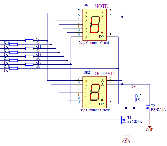
A 7 segment display has 8 inputs (for the 7 segments plus the dot). We need at least two displays (for the note and the octave). If we decide to represent the sharp and the flat symbols too, than we need three. But a flat note is just lower in pitch by a semitone which is the same as the sharp lower note, sharp being a higher pitch by a semitone. So actually we don’t need both sharp and flat symbols. And if we “represent” only the sharp we may use the dot (which we don’t need elsewhere) for this. A note with dot will be the note sharp. Of course we may use three 7 segment displays but there are some side effects. First: it will be wider. Bigger PCB, bigger case, maybe ugly proportions between width and length of the case. Second: to command two display we only need one IO which will drive both, alternating. But to drive three display we need at least two IOs. May be an issue. After all this considerations I decided to use two 7 segment displays. Driving both of them simultaneously will require 2 x 8 IO lines . But we only have 9 IOs. So we need to multiplex the two displays. We use the same 8 “data” lines for driving both and we switch alternatively each ON/OFF, taking care that the information present on the “data” lines corresponds to the momentarily ON display. By choosing a high switching rate, we trick the eye in believing that both are ON all the time, same as the movies or the television does. To switch ON/OFF we use the common line of the displays (each display consist of 8 LEDs with either all cathodes or all anodes connected together). As we will use common cathode display, we will drive the segments with voltage (high) and we will switch the ground of each display be means of a transistor. Using common cathode has the “advantage” that each line/bit which is high means the corresponding LED ON. If we had used the common anode than LEDs are ON for which the data is low. This may be confusing in HW prototyping and FW debugging, especially for newbies.
We will connect the transistors in a way that by switching one of them ON the other will be switch OFF and vice-versa (for rednecks: the other way round). I will use MOSFETs cause the voltage drop and therefore the power dissipation in the ON state is virtually zero. As they will be driven directly from the D1 mini board , they should have a gate threshold voltage of less then the HIGH level of the IOs (3.3V). I will use the BSN254A. It is an obsolete part, but it just happens that I have some of them laying on my desk.
Here is the solution. We drive directly from the D1 mini module the display and the transistors, by using 9 IOs.
Now, about displaying the deviation from the ideal note. The simplest way is to use three LEDs : a red one for pitch too low, a green one for tuned and a red one for pitch too high. This will require three additional command (IOs) line. But we have used already all of them for the Note/Octave display . We don’t have any available.
So back to start. We can’t drive the Note/Octave display directly from the D1 mini display. We have to use a serial transfer from the D1 mini module toward the display, instead this parallel one as above, in order to reduce the number of IOs used. For this we need to use some kind if IC which is able to transpose a stream of serial data in a parallel one. I wonder if something like this exists? Tam, tam, tam, tam, …. . I can release the tension and proudly announce that the CD4094 logic IC is doing exactly this.
The schematics look like this
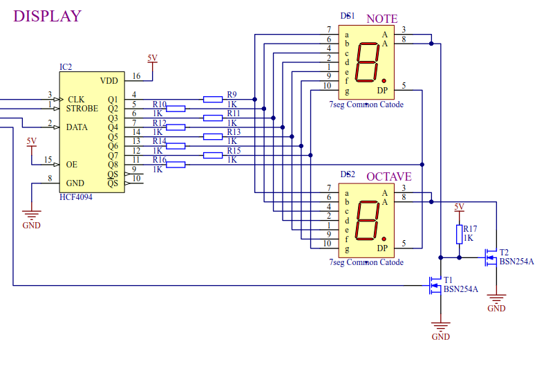
Now we need only 4 lines (and corresponding IOs) instead of 9, leaving enough IOs free for the tuning LEDs. As for any serial transfer we need a CLK line , a DATA line (on each CLK positive edge the DATA is transferred to the IC registers) and a STROBE line which we will set from LOW to HIGH as soon as all 8 DATA bits have been transferred, in order to change the parallel output of the IC to the new DATA byte. Data is flowing only from D1 mini module toward the IC and never the other way round. So, no need for a DataIn line, like in normal serial “communication”. This is just a serial transfer, not a communication both ways. As the CD4094 (in his STMicroelectronics commercial name of HCF4094) has to be supplied from 5V it will drive therefore the displays with the same 5V. The resistors between the HCF4094 outputs and the inputs of the 7 segments displays are defining the current through the LEDs and should be calculated for some mA to pass through them (and the LEDs). The current is depending on the specific display for a specific illumination, according data sheet. At 5V and LED forward voltage between 2V (for red and green LEDs) and 3.5V (for blue LEDs), the resistors are around (5-3)V / 2mA ≈ 1kΩ.
With the transistor T1 ON and therefore the Note display also ON, the gate voltage of T2 will be zero, and T2 and the Octave display will be OFF. As soon as T1 (and Note display) will be OFF, the resistor R17 will set the gate of T2 to 5V, turning it (and the Octave display) ON .
As for the tuning LEDs, as I said, we will drive them directly from the D1 mini.
Like this
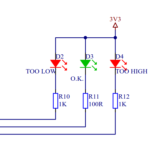
As the command lines are on the cathodes of the LEDs , the command logic should be inverse (IO LOW equals LED ON). I know that I just said above that this kind of driving may be confusing, but you confuse me if you niggas really think that I care that you are confused.
Note that we use 3.3V to supply the LEDs, cause the D1 mini outputs are 3.3V. If we had use 5V as supply , then the LED will still had a voltage drop of 5-3.3 = 1.7V, enough to turn it ON, even if the IO is HIGH , when the LED should be actually OFF. The resistors are determining the LEDs current. Same as above a 1kΩ is OK. Except for the green one. The green LED that I use needs more current than the red one for the same illumination and besides red is perceived by the human eye as more bright then green . Actually I did start with 1K for green too, but decided during the prototyping phase that for my device 100R will be better. (At least my eyes have seen red much brighter then green. And actually do we all see the same red? How do I know that you’r perception of the red color is the same as mine? Is the Matrix real?

Question after questions, but no time for answers.
Supply voltage
For those of you who don’t know yet, the guitar pedals are supplied with 9V DC, with a DC power jack (the 5.5mm outside diameter type), but with the negative on the inside pin. (Realy?).

As the pedals are usually connected together in a chain and sometimes they all use the same DC power supply we have to design our device to be use under the same conditions. We need to generate 5V out of the 9V input. The 5V will supplied to the D1 mini board and the display part. The 3.3V , generated inside the D1 mini , will be used for the tuning LEDs too. The D1 mini has a linear low drop voltage regulator IC (LDO) to generate 3.3V from the 5V. As we only need a couple of mA, we suppose that this will be OK and we will not burn the IC. The ESP8266 needs up some hundred of mA on 3.3V, and the LDO must deliver those 200-300mA. Therefore the additional 2mA for the LEDs, will do no harm.
It will be insane to use for the 9V to 5V conversion a linear regulator, as the maximum power disipation on it will be (9-5)V / 300mA = 1.3W. I am no environmentalist and I don’t want to save even the last electrons, but loosing 1.3W is insane. We should use a DC-DC buck converter. It’s a lot more efficient. And instead of designing a new one with a dedicated IC , we better use ready-to-go modules. Like this one
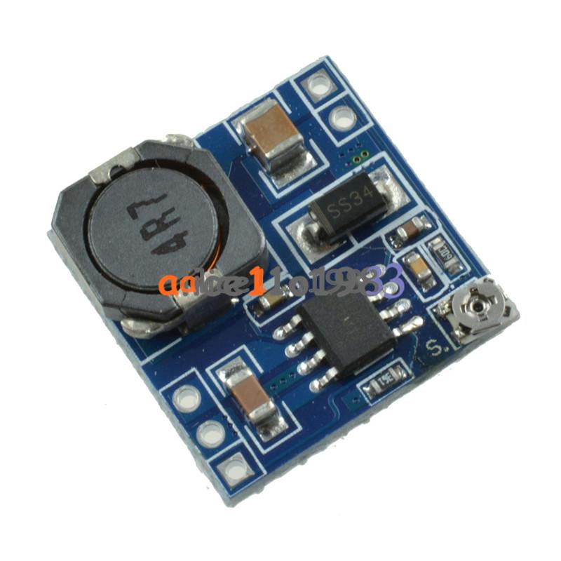
Input: 5-24V ; Output: 0.9-15V; Load current: max 2A . Very cheap but good enough as we only need 0.3A.
Other parts
Well , we are almost done. There was one more requirement on the device: to be truly bypass. Which means to let the guitar signal passing through, as it is and without any influence, as long as the device is shut off, and to cut the signal from passing through when we switch on and do the tuning (we don’t want to submit the audience to the pain of listening to the tuning sounds!). We need two audio jacks (6.3mm) one on each lateral side, with the input on the right side and the output left, cause this is the standard in the pedal business. (I swear that the input is right and not left, how it should be in every common sense device.) So, WTF guitar guys again!

I have told you, some moments ago as we have looked at the polarity of the supply jack, that the guitar guys are the wrong way around. (But is not as bad after all, as I am from Australia).
We need an ON/OFF switch which has three ON-OFF-ON switches inside in order to switch not only the supply but also the signal in the correct configuration. Besides, the switch must be a stump type one, cause it will be footled (handled with the foot).
Also a LED to indicate the presence of the 9V will be nice.
Finally , the schematics looks like this.
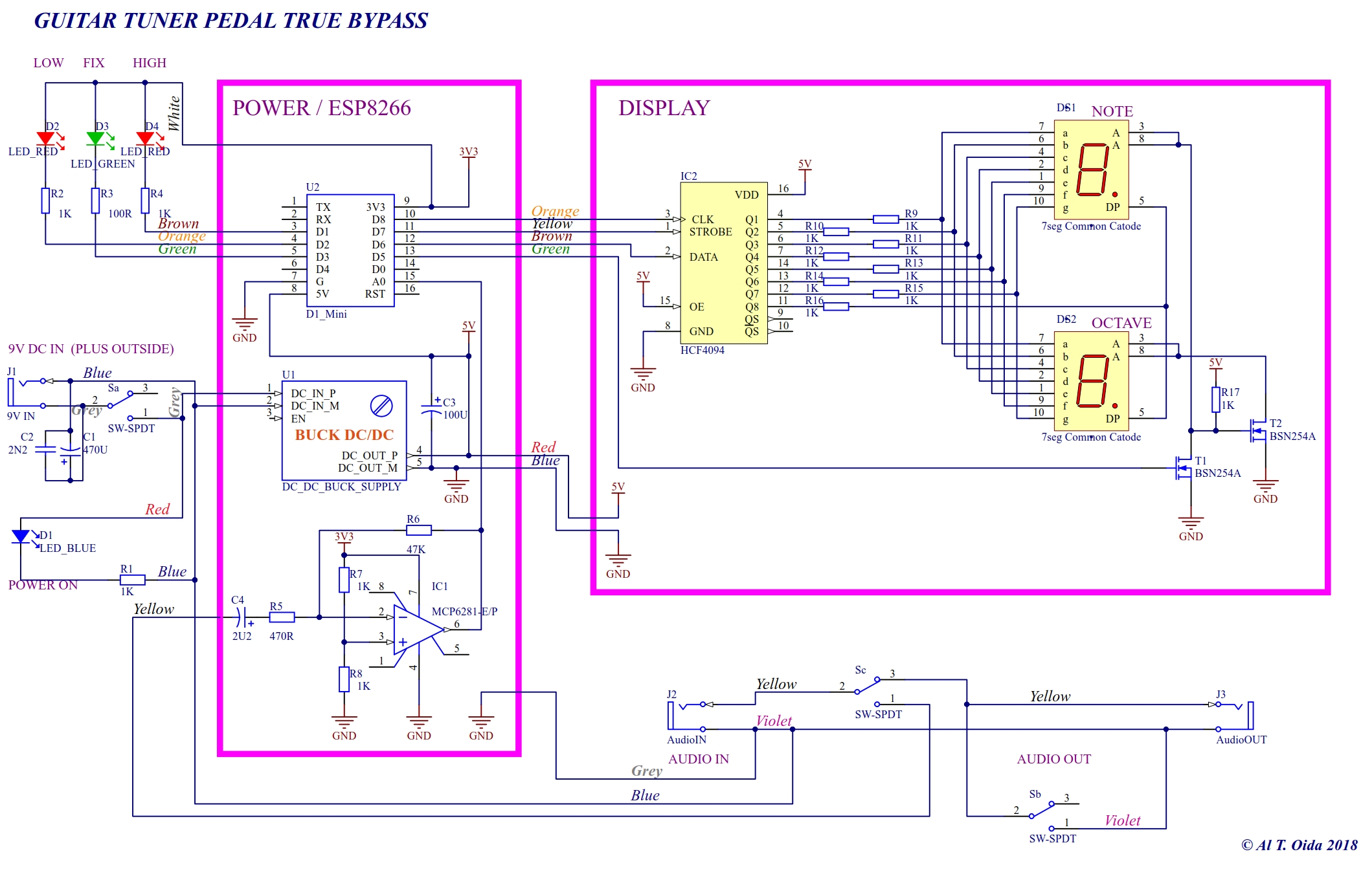
Based on this design I have build a prototype . On a breadboard.
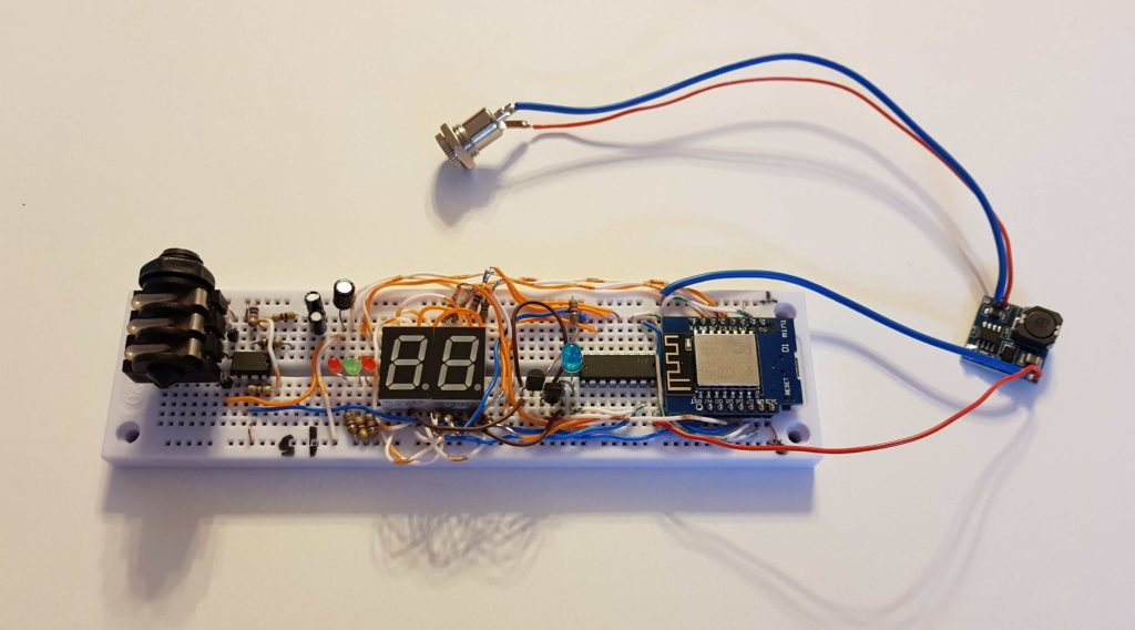
It is actually the same as the schematics. Only the audio jack for output and the stump switch are missing. Not relevant for prototype.
We will use this prototype to validate the hardware design and test the firmware.

.